
TEL:13526590898
 Scan to contact us
 Scan to view the mobile version

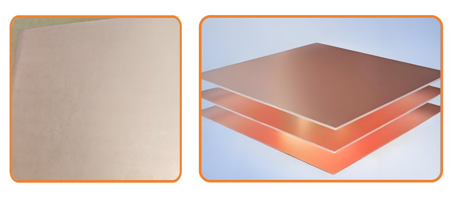
I. M9/M10 High-Frequency, High-Speed, High-Thermal-Conductivity, Low-Dk, Low-Df Copper-Clad Laminates (CCL)
Positioning: Premium PCB substrate for AI computing, supercomputing, and high-speed communications.
Key Advantages: Quartz-glass fabric + hydrocarbon resin system, supporting 224Gbps+ ultra-high-speed signal transmission. Paired with HVLP ultra-low-profile copper foil for superior signal integrity, excellent heat resistance, and high dimensional stability — ideal for high-end GPU/server PCBs.
II. Metallization of Diamond Substrates (via AMB or DPC)
1. Single-crystal and polycrystalline diamond
2. Copper-Diamond composite
3. Diamond-on-Silicon Carbide (SiC)
4. Diamond-on-Silicon Nitride (Si₃N₄)
5. Diamond-Silicon Carbide (SiC) composite
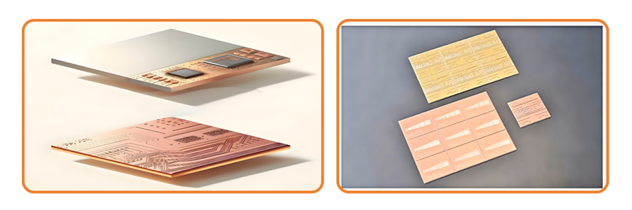
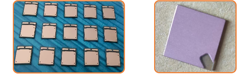
Base Substrate × Metallization Technology: DPC / AMB
Target Applications:SiC/GaN Power Modules, IGBTs, Energy Storage Converters (PCS), Automotive E-Drives, and Advanced Thermal Management for High-Speed Optical Modules.
Material Selection Guide:
▶For Maximum Thermal Conductivity: Single-Crystal & Polycrystalline Diamond + AMB/DPC
▶ For High-Reliability Power Applications: Diamond-on-SiC / Diamond-on-Si₃N₄ + AMB
▶For High-Frequency Fine-Line Routing: Polycrystalline Diamond / Diamond-on-SiC + DPC
▶ For Cost-Effective Mass Production: Diamond-on-SiC / Diamond-on-Si₃N₄ + DPC
▶ For Integrated Structural Thermal Management: Copper-Diamond Composite + Surface Plating